(China (Mainland))

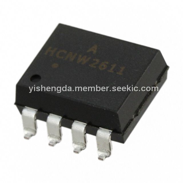
Product Summary
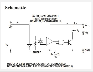
The HCNW2611 is an optically coupled gate that combine a GaAsP light emitting diode and an integrated high gain photo detector. An enable input allows the detector to be strobed. The output of the detector IC is an open collector Schottkyclamped transistor. The internal shield provides a guaranteed common mode transient immunity specification of 10,000 V/ms for the HCNW2611. This unique design provides maximum ac and dc circuit isolation while achieving TTL compatibility. The optocoupler ac and dc operational parameters are guaranteed from -40°C to +85°C allowing troublefree system performance. The HCNW2611 is suitable for high speed logic interfacing, input/output buffering, as line receivers in environments that conventional line receivers cannot tolerate and are recommended for use in extremely high ground or induced noise environments.
Parametrics
HCNW2611 absolute maximum ratings:(1)Storage Temperature, TS: -55 to 125℃; (2)Operating Temperature, TA: -40 to 85℃; (3)Average Forward Input Current, IF, Single 8-Pin DIP Single SO-8 Widebody: 20mA; (4)Average Forward Input Current, IF, Dual 8-Pin DIP Dual SO-8: 15mA; (5)Reverse Input Voltage, VR, 8-Pin DIP, SO-8: 5V; (6)Reverse Input Voltage, VR, Widebody: 3V; (7)Input Power Dissipation, PI, Widebody: 40mW; (8)Supply Voltage, VCC: 7V; (9)Enable Input Voltage (Not to Exceed VCC by more than 500 mV), VE, Single 8-Pin DIP Single SO-8 Widebody: VCC+0.5V; (10)Enable Input Current, IE: 5mA; (11)Output Collector Current, IO: 50mA; (12)Output Collector Voltage, VO: 7V; (13)Output Collector Power Dissipation, PO, Single 8-Pin DIP Single SO-8 Widebody: 85mW; (14)Output Collector Power Dissipation, PO, Dual 8-Pin DIP Dual SO-8: 60mW; (15)Lead Solder Temperature (Through Hole Parts Only), TLS, 8-Pin DIP: 260℃ for 10 sec. 1.6 mm below seating plane.
Features
HCNW2611 features: (1)5 kV/ms Minimum Common Mode Rejection (CMR) at VCM = 1000 V for HCPLX611/X661, HCNW2611; (2)High Speed: 10 MBd Typical; (3)LSTTL/TTL Compatible; (4)Low Input Current Capability: 5 mA; (5)Guaranteed ac and dc Performance over Temperature: -40°C to +85°C; (6)Available in 8-Pin DIP, SOIC-8, Widebody Packages; (7)Strobable Output (Single Channel Products Only); (8)Safety Approval; (9)MIL-STD-1772 Version Available .
Diagrams
| Image | Part No | Mfg | Description |  |
Pricing (USD) |
Quantity | ||||||||||||
|---|---|---|---|---|---|---|---|---|---|---|---|---|---|---|---|---|---|---|
 |
 HCNW2611 |
Avago Technologies |
High Speed Optocouplers 10MBd 1Ch 5mA |
Data Sheet |
|
|
||||||||||||
|
HCNW2611#300 |
Avago Technologies |
High Speed Optocouplers 10MBd 1Ch 5mA |
Data Sheet |
|
|
||||||||||||
|
HCNW2611-300E |
Avago Technologies |
High Speed Optocouplers 10MBd 1Ch 5mA |
Data Sheet |
|
|
||||||||||||
|
HCNW2611-000E |
Avago Technologies |
High Speed Optocouplers 10MBd 1Ch 5mA |
Data Sheet |
|
|
||||||||||||
|
HCNW2611-500E |
Avago Technologies |
High Speed Optocouplers 10MBd 1Ch 5mA |
Data Sheet |
|
|
||||||||||||
|
HCNW2611#500 |
Avago Technologies |
High Speed Optocouplers 10MBd 1Ch 5mA |
Data Sheet |
|
|
||||||||||||